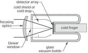
This was the second of a pair of closely related innovations, improving the calibration process for cryogenically-cooled and vacuum-sealed infrared detector arrays, as used in the missile guidance sensor illustrated at right.
The detector arrays, which were doped semiconductors, were made onsite at an in-house foundry. One of the final steps before assembling a detector array into a sensor was to calibrate its performance under cryogenic operating conditions.
The first innovation, the Partitioning Algorithm, generated random lists of detector pixels to be tested at a given current, and after each test new lists would be generated until all pixels were calibrated. Each list was essentially random, representing the variability in any given foundry batch from which the detectors were harvested.
This algorithm, the Optimal Switching Algorithm, responded to these random lists of pixels by determining the minimum-time test sequence for the remaining uncalibrated pixels.
Together, these algorithms provided ways to simultaneously 1) minimize the number of bias current test values, and 2) minimize the number of tests required on each pixel. Both are “minimized” in the sense of providing performance equivalent to binary search.
A final heuristic refinement adjusted the search intervals based on the difference between measured response and desired response, rather than halving as in traditional binary search.